# Transistor
## Microsim
<iframe src="https://editor.p5js.org/sciencenibber/full/C1jNqYHch" width="100%" height="620" frameborder="0" sandbox="allow-scripts allow-same-origin"></iframe>
<img src="../ENGINES_Electrical-Engineering_Images/Transistor.png" alt="Transistor microsim">
[Open in the p5.js editor](https://editor.p5js.org/sciencenibber/sketches/C1jNqYHch)
```js
// Transistor - the three-terminal active device that lets a small control signal
// command a large current: amplifier and switch in one. Illustrated through the
// canonical BJT common-emitter OUTPUT CHARACTERISTICS -- a family of I_C-V_CE curves
// indexed by base current I_B -- with a load line whose intersection with the selected
// curve is the operating point Q, walked from cutoff through active to saturation.
// Wikitube / E.N.G.I.N.E.S. hub -> Electrical engineering room. One file, one ARTICLE.
//
// LEARNING OBJECTIVE
// Predict, from I_C = beta*I_B and the load line I_C = (V_CC - V_CE)/R_C, WHERE the
// operating point Q sits for a given base drive, and explain how raising I_B walks Q
// up the load line through the three regions -- cutoff (open switch, I_C ~ 0), active
// (amplifier, Av = -gm*(R_C||r_o) largest near mid-line), and saturation (closed
// switch, V_CE ~ 0) -- so the same device is both a linear amplifier and a digital
// switch depending only on its bias.
//
// PATTERN chart-frame output characteristics (the star) -- collector current I_C on an
// auto-scaled linear axis vs collector-emitter voltage V_CE on a fixed linear axis
// (0 .. 16 V). A faint family of curves (I_B = 0,20,...,120 uA) is drawn as single
// paths; the SELECTED-I_B curve is drawn bright with its plateau shaded; over it a
// straight amber load line I_C=(V_CC-V_CE)/R_C, whose intersection with the selected
// curve is the operating point Q (crosshair to both axes). Faint swing ghosts at
// I_B +/- dI_B show the small-signal excursion. Composed with a Pattern A annotated
// NPN common-emitter schematic.
//
// MODEL closed-form output characteristic + a numeric load-line solve.
// I_C(V_CE; I_B) = beta*I_B * (1 - exp(-V_CE/V_CEsat)) * (1 + V_CE/V_A)
// (1 - exp(-V_CE/V_CEsat)) knee: 0 at V_CE=0 -> 1 within a few V_CEsat (~0.2 V)
// (1 + V_CE/V_A) Early effect: plateau tilt; r_o = V_A/I_C
// load: I_C = (V_CC - V_CE)/R_C KVL line: x-int V_CC, y-int V_CC/R_C
// Q: root of I_C(V_CE) - (V_CC - V_CE)/R_C = 0 by fixed-count bisection on
// V_CE in [0, V_CC] (the char. is monotonic up, the line monotonic down ->
// a single sign change -> no runaway-loop risk)
// gm = I_C/V_T, r_o = V_A/I_C, Av = -gm*(R_C || r_o), P_C = V_CE*I_C
// No time integration (the device is memoryless / resistive): no dt, no Verlet, and
// NO per-frame inner loop over a system state. SI units internally (A, V, ohm); the
// base current is in uA and R_C is log-mapped, converting at the input only.
//
// EDITOR-SAFE noLoop()+redraw(), input-driven; the panel frames, the fixed V_CE-axis
// gridlines/labels, the axis titles and the schematic RAILS are baked ONCE into an
// offscreen buffer; draw() runs only fixed-length loops (a few hundred curve samples
// drawn as ONE path per curve, ~7 family curves, ~7 current-axis ticks, a handful of
// schematic primitives) clipped to the plot rect; ASCII-only strings (Golden Rule 6);
// p5.disableFriendlyErrors = true. Top-level names avoid p5 globals AND p5 method
// names (no scale, mag, pow, log, exp, map, ratio, split, ...; the current gain is
// named gainHFE, NOT beta): the model uses Math.* and bespoke xForV / yForI mappers.
const ARTICLE = "Transistor";
const TITLE = "Transistor: BJT output characteristics, load line, and the Q-point walk";
const WIKI = "en.wikitube.io/wiki/" + ARTICLE;
// ---------- physical / model constants (SI) ----------
const KB = 1.380649e-23; // Boltzmann constant (J/K)
const QE = 1.602176634e-19; // elementary charge (C)
const TEMP_K = 300; // room temperature (K)
const VT = KB * TEMP_K / QE; // thermal voltage kT/q ~ 0.02585 V
const VA_EARLY = 80; // Early voltage V_A (V): plateau tilt + r_o = V_A/I_C
const VCESAT = 0.20; // knee scale (V): width of the saturation->active rise
const DIB_SWING_UA = 4; // small-signal base-current excursion for the ghosts (uA)
// ---------- state: single source of truth, mirrored by the controls ----------
let baseUA = 40; // uA base current I_B (the control/input)
let gainHFE = 150; // - DC current gain beta = hFE (named gainHFE: avoid p5 'beta')
let supplyV = 10; // V collector supply V_CC
let loadR = 1000; // ohm collector load resistor R_C
// ---------- defaults (reset restores ALL state, Golden Rule 4) ----------
const D_IB = 40, D_HFE = 150, D_VCC = 10, D_R = 1000;
// ---------- chart axis constants ----------
const VCEMIN = 0.0; // V voltage-axis floor (fixed)
const VCEMAX = 16.0; // V voltage-axis ceiling (fixed; covers V_CC <= 15)
const NSAMP = 180; // samples per characteristic curve (fixed; one polyline)
const IB_FAMILY = [0, 20, 40, 60, 80, 100, 120]; // uA: the faint reference family
let iLo, iHi; // A current-axis bounds (auto-scaled each redraw)
// ---------- layout (computed from width/height; never hard-coded) ----------
let devX, devY, devW, devH; // schematic panel
let panX, panY, panW, panH; // readout panel
let rcX, rcY, rcW, rcH; // I_C-V_CE chart panel
let ctrlY; // control region top
let cc1, cc2, cc3, cc4; // control column x positions
let plotX0, plotY0, plotW, plotH; // chart plot rectangle (plotY0 = bottom)
// ---------- p5 objects ----------
let staticBuf; // baked static background buffer
let ibSlider, hfeSlider, vccSlider, rSlider, resetButton;
// ---------- palette (built once) ----------
let COL;
function setup() {
createCanvas(720, 520);
pixelDensity(2);
p5.disableFriendlyErrors = true; // Golden Rule 8: zero FES noise
computeLayout();
buildPalette();
staticBuf = createGraphics(width, height);
bakeScene(staticBuf); // frames + V_CE axis + titles + rails, once
// --- controls: linear sliders read directly; R_C is log-mapped via 0..120 steps ---
ibSlider = createSlider(0, 120, D_IB, 1); // I_B 0 .. 120 uA
hfeSlider = createSlider(20, 400, D_HFE, 5); // beta 20 .. 400
vccSlider = createSlider(1, 15, D_VCC, 0.5); // V_CC 1 .. 15 V
rSlider = createSlider(0, 120, Math.round(rToSlider(D_R)), 1); // R_C 100 ohm .. 10 kohm (log)
ibSlider.position(cc1, ctrlY + 18); ibSlider.style('width', '150px');
hfeSlider.position(cc2, ctrlY + 18); hfeSlider.style('width', '150px');
vccSlider.position(cc3, ctrlY + 18); vccSlider.style('width', '150px');
rSlider.position(cc1, ctrlY + 52); rSlider.style('width', '150px');
ibSlider.input(onCtrl); hfeSlider.input(onCtrl);
vccSlider.input(onCtrl); rSlider.input(onCtrl);
resetButton = createButton('Reset');
resetButton.position(cc4, ctrlY + 50);
resetButton.mousePressed(resetAll);
noLoop(); // input-driven from here on
}
function computeLayout() {
const drawH = height * 0.78; // top drawing region (~405 px)
const top = 42;
devX = 16; devY = top; devW = width * 0.52 - devX; devH = 168;
panX = devX + devW + 14; panY = top;
panW = width - panX - 14; panH = 168;
rcX = 16; rcY = top + devH + 14;
rcW = width - 32; rcH = drawH - rcY - 12;
ctrlY = drawH + 4;
cc1 = 16; cc2 = 190; cc3 = 364; cc4 = 538;
// chart plot rectangle: left 56 for current labels, right 16 margin
plotX0 = rcX + 56; plotY0 = rcY + rcH - 26;
plotW = rcW - 56 - 16; plotH = rcH - 14 - 26;
}
function buildPalette() {
COL = {
bg: color('#0b0f16'),
panel: color('#111a26'),
panelEdge: color(64, 80, 102),
text: color('#e8eef6'),
muted: color('#93a0b2'),
wire: color('#7f8ea3'), // connecting wire
res: color('#d98a4a'), // resistor (warm)
npn: color('#5ad1ff'), // transistor symbol (cyan)
src: color('#c792ea'), // supply / source (violet)
grid: color(54, 66, 84),
axis: color(120, 138, 160), // emphasized zero axes
fam: color(99, 122, 150, 90), // faint family curves
curve: color('#4dd0a8'), // selected output curve (mint)
curveFill: color(77, 208, 168, 26), // active-plateau shading
load: color('#ffae57'), // load line (amber)
qpt: color('#ffd166'), // operating-point marker (yellow)
ghost: color(255, 209, 102, 150), // small-signal swing ghosts
flow: color('#5ee08c'), // current-flow arrow
warn: color('#ff5252'),
good: color('#5ee08c'),
gauge: color('#ffd166')
};
}
// ============== slider transform: R_C log scale over 100 ohm .. 10 kohm (2 decades) ==============
function rToSlider(v) { return (Math.log(v) / Math.LN10 - 2) / 2 * 120; }
function sliderToR(s) { return Math.pow(10, 2 + (s / 120) * 2); }
// =================== device model (smooth output characteristic + load line) ===================
// Collector current of the common-emitter BJT for base current ibA (A) and gain hfe.
// Monotonic increasing in vce: knee factor up, Early factor up. Returns 0 for vce<=0.
function charIc(vce, ibA, hfe) {
if (vce <= 0) return 0;
return hfe * ibA * (1 - Math.exp(-vce / VCESAT)) * (1 + vce / VA_EARLY);
}
// Operating-point V_CE: root of charIc(vce) - (V_CC - vce)/R_C = 0 by bracketed bisection.
// f(0) = -V_CC/R_C < 0 ; f(V_CC) = charIc(V_CC) >= 0 ; monotone -> a single root in [0,V_CC].
function operatingVce(ibA, hfe) {
let lo = 0, hi = Math.max(supplyV, 1e-3);
for (let k = 0; k < 60; k++) {
const mid = (lo + hi) / 2;
const f = charIc(mid, ibA, hfe) - (supplyV - mid) / loadR;
if (f > 0) hi = mid; else lo = mid;
}
return (lo + hi) / 2;
}
function solveBJT() {
const ibA = baseUA * 1e-6;
const vq = operatingVce(ibA, gainHFE);
const ic = Math.max((supplyV - vq) / loadR, 0); // load-line current at Q (== device I_C)
const scI = supplyV / loadR; // short-circuit / closed-switch current
const vrc = ic * loadR; // drop across R_C (= V_CC - V_CE)
const icPlat = gainHFE * ibA; // ideal active plateau beta*I_B
const gm = ic / VT; // transconductance (S)
const ro = ic > 1e-9 ? VA_EARLY / ic : 1e12; // output resistance (ohm)
const rpar = (loadR * ro) / (loadR + ro); // R_C || r_o
const av = -gm * rpar; // CE small-signal voltage gain
const pc = vq * ic; // collector power dissipation
const alphaCB = gainHFE / (gainHFE + 1); // common-base current gain (alphaCB: avoid p5 'alpha')
// region classification (read off Q)
let reg;
if (baseUA < 0.5 || ic < 5e-6) reg = "cutoff";
else if (vq < 0.30) reg = "saturation";
else reg = "active";
// small-signal swing ghosts (operating points at I_B +/- dI_B)
const dIbA = DIB_SWING_UA * 1e-6;
const vqP = operatingVce(ibA + dIbA, gainHFE);
const icP = Math.max((supplyV - vqP) / loadR, 0);
const vqM = operatingVce(Math.max(ibA - dIbA, 0), gainHFE);
const icM = Math.max((supplyV - vqM) / loadR, 0);
return { vq: vq, ic: ic, scI: scI, vrc: vrc, icPlat: icPlat, gm: gm, ro: ro,
rpar: rpar, av: av, pc: pc, alpha: alphaCB, reg: reg,
vqP: vqP, icP: icP, vqM: vqM, icM: icM };
}
// nice round ceiling (1/2/5 x 10^k) for the auto-scaled current axis
function niceCeil(x) {
if (x <= 0) return 1;
const e = Math.floor(Math.log(x) / Math.LN10);
const f = x / Math.pow(10, e);
let m = 10;
if (f <= 1) m = 1; else if (f <= 2) m = 2; else if (f <= 5) m = 5;
return m * Math.pow(10, e);
}
// =============================== DRAW ===============================
function draw() {
background(COL.bg);
image(staticBuf, 0, 0);
const s = solveBJT();
// auto-scale the current axis to the load line + operating point (the family curves'
// plateaus can exceed this: they are clipped to the plot, exactly like the diode)
iHi = niceCeil(1.15 * Math.max(s.ic, s.scI, 1e-3));
iLo = -0.05 * iHi;
drawChart(s);
drawSchematic(s);
drawReadout(s);
drawHUD(s);
}
// ---------- static scenery baked once into an offscreen buffer ----------
function bakeScene(g) {
g.push();
g.background(COL.bg);
panelRect(g, devX, devY, devW, devH, "Circuit: NPN common-emitter (V_CC + R_C + transistor)");
panelRect(g, panX, panY, panW, panH, ""); // "Readouts" title drawn live
panelRect(g, rcX, rcY, rcW, rcH, "Output characteristics: I_C vs V_CE family + load line");
bakeVAxis(g); // fixed V_CE axis + titles
g.pop();
}
function panelRect(g, x, y, w, h, title) {
g.noStroke(); g.fill(COL.panel); g.rect(x, y, w, h, 8);
g.noFill(); g.stroke(COL.panelEdge); g.strokeWeight(1); g.rect(x, y, w, h, 8);
if (title.length > 0) {
g.noStroke(); g.fill(COL.muted); g.textSize(11); g.textAlign(LEFT, BOTTOM);
g.text(title, x + 4, y - 3);
}
}
// fixed V_CE-axis gridlines + labels + axis titles (baked once)
function bakeVAxis(g) {
g.push();
g.textSize(8.5);
for (let v = 0; v <= 16; v += 2) {
const gx = plotX0 + (v - VCEMIN) / (VCEMAX - VCEMIN) * plotW;
const zero = (v === 0);
g.stroke(zero ? COL.axis : COL.grid); g.strokeWeight(zero ? 1.6 : 1);
g.line(gx, plotY0 - plotH, gx, plotY0);
g.noStroke(); g.fill(zero ? COL.text : COL.muted);
g.textAlign(CENTER, TOP); g.text(v, gx, plotY0 + 5);
}
// axis titles
g.noStroke(); g.fill(COL.muted); g.textSize(9.5); g.textAlign(CENTER, TOP);
g.text("collector-emitter voltage V_CE (V)", plotX0 + plotW / 2, plotY0 + 18);
g.push(); g.translate(rcX + 14, plotY0 - plotH / 2); g.rotate(-HALF_PI);
g.textAlign(CENTER, CENTER); g.fill(COL.curve); g.text("collector current I_C", 0, 0); g.pop();
g.pop();
}
// =============================== CHART (output characteristics + load line) ===============================
function xForV(v) { return plotX0 + (v - VCEMIN) / (VCEMAX - VCEMIN) * plotW; }
function yForI(i) { return plotY0 - (constrain(i, iLo, iHi) - iLo) / (iHi - iLo) * plotH; }
// one characteristic curve for base current ibUA (uA), drawn as a single path.
function curvePath(ibUA) {
const ibA = ibUA * 1e-6;
beginShape();
for (let i = 0; i <= NSAMP; i++) {
const v = VCEMIN + (i / NSAMP) * (VCEMAX - VCEMIN);
vertex(xForV(v), yForI(charIc(v, ibA, gainHFE)));
}
endShape();
}
function drawChart(s) {
// --- live current-axis gridlines + labels (auto-scaled) ---
push();
textSize(8.5);
const step = niceCeil(iHi / 5);
const kLo = Math.ceil(iLo / step + 1e-9);
const kHi = Math.round(iHi / step);
for (let k = kLo; k <= kHi; k++) {
const iv = k * step;
const gy = yForI(iv);
const zero = (k === 0);
stroke(zero ? COL.axis : COL.grid); strokeWeight(zero ? 1.6 : 1);
line(plotX0, gy, plotX0 + plotW, gy);
noStroke(); fill(zero ? COL.text : COL.muted); textAlign(RIGHT, CENTER);
text(fmtAmp(iv), plotX0 - 6, gy);
}
pop();
// everything data-dependent is clipped to the plot rectangle
push();
drawingContext.save();
drawingContext.beginPath();
drawingContext.rect(plotX0, plotY0 - plotH, plotW, plotH);
drawingContext.clip();
// --- faint reference family (single plain paths, no shadow) ---
noFill(); stroke(COL.fam); strokeWeight(1.2);
for (let f = 0; f < IB_FAMILY.length; f++) {
if (Math.abs(IB_FAMILY[f] - baseUA) < 0.6) continue; // skip the one we draw bright
curvePath(IB_FAMILY[f]);
}
// family labels at the right edge (only the topmost few, to avoid clutter)
noStroke(); fill(COL.fam); textAlign(RIGHT, BOTTOM); textSize(8);
for (let f = 0; f < IB_FAMILY.length; f++) {
const yEnd = yForI(charIc(VCEMAX, IB_FAMILY[f] * 1e-6, gainHFE));
if (yEnd > plotY0 - plotH + 6 && yEnd < plotY0 - 2)
text(IB_FAMILY[f] + "uA", plotX0 + plotW - 2, yEnd);
}
// --- selected curve: plateau shading (area under) then the bright glowing path ---
const ibA = baseUA * 1e-6;
noStroke(); fill(COL.curveFill);
beginShape();
vertex(xForV(VCEMIN), yForI(0));
for (let i = 0; i <= NSAMP; i++) {
const v = VCEMIN + (i / NSAMP) * (VCEMAX - VCEMIN);
vertex(xForV(v), yForI(charIc(v, ibA, gainHFE)));
}
vertex(xForV(VCEMAX), yForI(0));
endShape(CLOSE);
drawingContext.save();
drawingContext.shadowBlur = 8;
drawingContext.shadowColor = 'rgba(77,208,168,0.7)';
noFill(); stroke(COL.curve); strokeWeight(2.6); strokeJoin(ROUND);
curvePath(baseUA); // ONE path under one shadow setting
drawingContext.restore();
// --- load line: I_C = (V_CC - V_CE)/R_C, from (0, V_CC/R_C) to (V_CC, 0) ---
stroke(COL.load); strokeWeight(2);
line(xForV(0), yForI(s.scI), xForV(supplyV), yForI(0));
noStroke(); fill(COL.load); textAlign(LEFT, TOP); textSize(9);
text("load line I_C=(V_CC-V_CE)/R_C", plotX0 + 6, plotY0 - plotH + 3);
// --- small-signal swing ghosts (active region only) ---
if (s.reg === "active") {
const xP = xForV(s.vqP), yP = yForI(s.icP);
const xM = xForV(s.vqM), yM = yForI(s.icM);
stroke(COL.ghost); strokeWeight(1.2); drawingContext.setLineDash([2, 3]);
line(xP, yP, xM, yM); drawingContext.setLineDash([]);
noStroke(); fill(COL.ghost);
circle(xP, yP, 6); circle(xM, yM, 6);
textAlign(LEFT, BOTTOM); textSize(8);
text("I_B swing", Math.min(xP, xM) - 2, Math.min(yP, yM) - 4);
}
// --- operating point Q at the intersection, with crosshair to both axes ---
const ox = xForV(s.vq), oy = yForI(s.ic);
stroke(COL.qpt); strokeWeight(1); drawingContext.setLineDash([3, 3]);
line(ox, oy, ox, plotY0); // down to V_CE axis
line(ox, oy, plotX0, oy); // left to I_C axis
drawingContext.setLineDash([]);
stroke(COL.bg); strokeWeight(1.5); fill(COL.qpt); circle(ox, oy, 10);
noStroke(); fill(COL.qpt); textAlign(LEFT, BOTTOM); textStyle(BOLD); textSize(11);
text("Q", ox + 8, oy - 3); textStyle(NORMAL);
// --- region corner cues ---
noStroke(); textSize(8.5);
fill(COL.warn); textAlign(RIGHT, BOTTOM);
text("cutoff (switch open)", xForV(VCEMAX) - 4, plotY0 - 4);
fill(COL.gauge); textAlign(LEFT, TOP);
text("sat (switch closed)", xForV(0) + 4, plotY0 - plotH + 16);
drawingContext.restore();
pop();
}
// =============================== SCHEMATIC (Pattern A: NPN common-emitter) ===============================
function drawSchematic(s) {
const sLeft = devX + 40; // base-drive column
const sMid = devX + devW * 0.56; // transistor base-bar x
const sTermX = sMid + 22; // collector/emitter terminal x (vertical wire)
const sTopY = devY + 40; // V_CC rail y
const sBotY = devY + devH - 30; // ground node y
const barY = (sTopY + sBotY) / 2 + 8; // base-bar centre y
const barHalf = 15;
const colJoinY = barY - barHalf - 6; // collector terminal (top of vertical wire)
const emJoinY = barY + barHalf + 6; // emitter terminal (top of emitter wire)
push();
// --- V_CC rail + supply node ---
stroke(COL.wire); strokeWeight(2); strokeCap(ROUND);
line(sTermX - 26, sTopY, sTermX, sTopY);
noStroke(); fill(COL.src); circle(sTermX, sTopY, 5);
noStroke(); fill(COL.src); textAlign(RIGHT, CENTER); textSize(10);
text("+V_CC " + fmtVolt(supplyV), sTermX - 30, sTopY);
// --- collector load resistor R_C (vertical) between rail and collector ---
stroke(COL.wire); strokeWeight(2);
// (R_C body drawn by drawResistorV; leads handled there)
pop();
drawResistorV(sTermX, sTopY, colJoinY, COL.res);
push();
stroke(COL.wire); strokeWeight(2); strokeCap(ROUND);
// collector vertical wire below R_C down to the collector join
// (drawResistorV already drew to colJoinY top; continue to the transistor join)
// emitter wire down to ground
line(sTermX, emJoinY, sTermX, sBotY);
pop();
// --- transistor symbol (NPN): base bar + collector/emitter diagonal stubs ---
push();
// enclosing circle
noFill(); stroke(COL.npn); strokeWeight(1.2);
circle(sMid + 8, barY, (barHalf + 10) * 2);
// base bar
stroke(COL.npn); strokeWeight(2.6); strokeCap(ROUND);
line(sMid, barY - barHalf, sMid, barY + barHalf);
// base lead (from the left)
stroke(COL.wire); strokeWeight(2);
line(sLeft + 12, barY, sMid, barY);
// collector stub: bar -> collector terminal (up-right)
stroke(COL.npn); strokeWeight(2.4);
line(sMid, barY - barHalf * 0.45, sTermX, colJoinY);
// emitter stub: bar -> emitter terminal (down-right) with NPN arrowhead (points out)
line(sMid, barY + barHalf * 0.45, sTermX, emJoinY);
// arrowhead on the emitter, pointing along the stub away from the base
const ax = sTermX, ay = emJoinY;
const dx = sTermX - sMid, dy = emJoinY - (barY + barHalf * 0.45);
const dlen = Math.sqrt(dx * dx + dy * dy);
const ux = dx / dlen, uy = dy / dlen;
const px = -uy, py = ux;
noStroke(); fill(COL.npn);
triangle(ax, ay, ax - 8 * ux + 4 * px, ay - 8 * uy + 4 * py,
ax - 8 * ux - 4 * px, ay - 8 * uy - 4 * py);
pop();
// --- base current source (a circle with a right arrow) feeding the base ---
push();
noFill(); stroke(COL.gauge); strokeWeight(1.6);
circle(sLeft, barY, 20);
stroke(COL.gauge); strokeWeight(1.8); strokeCap(ROUND);
line(sLeft - 5, barY, sLeft + 5, barY);
noStroke(); fill(COL.gauge);
triangle(sLeft + 5, barY, sLeft + 1, barY - 3, sLeft + 1, barY + 3);
pop();
// --- ground symbol at the emitter foot ---
drawGround(sTermX, sBotY, COL.wire);
// --- current-flow arrow on the collector wire (size/brightness track I_C) ---
const mag = Math.min(s.ic / Math.max(s.scI, 1e-9), 1);
if (s.ic > 1e-6) {
drawFlowArrow(sTermX, (sTopY + colJoinY) / 2, COL.flow, 0.35 + 0.65 * mag);
}
// --- V_CE bracket on the right between collector and emitter terminals ---
push();
stroke(COL.qpt); strokeWeight(1.2); strokeCap(ROUND);
const bx = sTermX + 16;
line(bx, colJoinY, bx, emJoinY);
line(bx - 3, colJoinY, bx + 3, colJoinY);
line(bx - 3, emJoinY, bx + 3, emJoinY);
noStroke(); fill(COL.qpt); textAlign(LEFT, CENTER); textSize(9.5);
text("V_CE=" + fmtVolt(s.vq), bx + 6, (colJoinY + emJoinY) / 2);
pop();
// --- labels ---
push(); noStroke(); textSize(10);
fill(COL.res); textAlign(LEFT, CENTER);
text("R_C " + fmtOhm(loadR), sTermX + 8, (sTopY + colJoinY) / 2 - 8);
fill(COL.flow); textAlign(LEFT, CENTER); textSize(9.5);
text("I_C=" + fmtAmp(s.ic), sTermX + 8, (sTopY + colJoinY) / 2 + 8);
fill(COL.npn); textAlign(CENTER, TOP); textSize(10);
text("NPN", sMid + 8, barY + barHalf + 12);
fill(COL.gauge); textAlign(CENTER, TOP); textSize(9.5);
text("I_B=" + fmtAmpUA(baseUA), (sLeft + sMid) / 2, barY + 8);
pop();
}
// collector load resistor as a vertical zig-zag drawn as ONE path, with leads
function drawResistorV(cx, yTop, yBot, col) {
const zz = (yBot - yTop) * 0.56, z0 = (yTop + yBot) / 2 - zz / 2;
const n = 6, amp = 6, stp = zz / n;
push(); stroke(col); strokeWeight(2.4); strokeCap(ROUND); noFill();
line(cx, yTop, cx, z0);
beginShape();
vertex(cx, z0);
for (let i = 0; i < n; i++) vertex(cx + (i % 2 === 0 ? -amp : amp), z0 + stp * (i + 0.5));
vertex(cx, z0 + zz);
endShape();
line(cx, z0 + zz, cx, yBot);
pop();
}
// ground symbol (three shrinking horizontal bars) at the foot of a vertical wire
function drawGround(cx, cy, col) {
push(); stroke(col); strokeWeight(2); strokeCap(ROUND);
line(cx, cy, cx, cy + 6);
line(cx - 10, cy + 6, cx + 10, cy + 6);
line(cx - 6, cy + 10, cx + 6, cy + 10);
line(cx - 2, cy + 14, cx + 2, cy + 14);
pop();
}
// small downward current-flow arrow on a vertical wire; a = alpha 0..1
function drawFlowArrow(cx, cy, col, a) {
push();
const c = color(red(col), green(col), blue(col), 255 * a);
stroke(c); strokeWeight(2.2); strokeCap(ROUND);
line(cx, cy - 10, cx, cy + 6);
noStroke(); fill(c);
triangle(cx, cy + 12, cx - 4, cy + 4, cx + 4, cy + 4); // points DOWN (conventional I_C)
pop();
}
// =============================== READOUT PANEL ===============================
function drawReadout(s) {
push();
textAlign(LEFT, TOP); noStroke();
const x = panX + 12; let y = panY + 10;
fill(COL.text); textStyle(BOLD); textSize(13); text("Readouts", x, y); y += 18;
fill(COL.npn); textStyle(BOLD); textSize(11.5);
text("NPN BJT common-emitter", x, y); y += 16;
textStyle(NORMAL); textSize(10.5); fill(COL.muted);
text("beta = " + nf(gainHFE, 1, 0) + " alpha = " + nf(s.alpha, 1, 3), x, y); y += 14;
fill(COL.muted); text("I_C(active) = beta*I_B = ", x, y);
fill(COL.text); text(fmtAmp(s.icPlat), x + 152, y); y += 14;
fill(COL.muted); text("V_T = kT/q = " + fmtVolt(VT) + " V_A = " + nf(VA_EARLY,1,0) + " V", x, y); y += 18;
fill(COL.qpt); textStyle(BOLD); textSize(13.5); text("Operating point Q", x, y);
textStyle(NORMAL); textSize(11); y += 17;
fill(COL.muted); text("V_CE =", x, y); fill(COL.text); text(fmtVolt(s.vq), x + 48, y);
fill(COL.muted); text("I_C =", x + 132, y); fill(COL.text); text(fmtAmp(s.ic), x + 170, y); y += 15;
fill(COL.muted); text("V_RC = I_C*R_C", x, y); fill(COL.text); text(fmtVolt(s.vrc), x + 110, y); y += 14;
fill(COL.muted); text("P_C = V_CE*I_C", x, y); fill(COL.text); text(fmtWatt(s.pc), x + 110, y); y += 16;
const rl = regionLabel(s);
fill(rl.c); textStyle(BOLD); textSize(11.5); text(rl.t, x, y); textStyle(NORMAL); y += 18;
fill(COL.curve); textStyle(BOLD); textSize(12); text("Small-signal (at Q)", x, y);
textStyle(NORMAL); textSize(10.5); y += 15;
fill(COL.muted); text("gm = I_C/V_T =", x, y); fill(COL.text); text(fmtSiemens(s.gm), x + 110, y); y += 14;
fill(COL.muted); text("r_o = V_A/I_C =", x, y); fill(COL.text); text(fmtOhm(s.ro), x + 110, y); y += 14;
fill(COL.muted); text("Av = -gm(R_C||r_o) =", x, y);
fill(s.reg === "active" ? COL.good : COL.muted);
text(s.reg === "active" ? fmtGain(s.av) : "-- (not active)", x + 138, y); y += 16;
fill(COL.load); textStyle(BOLD); textSize(11.5);
text("load line corners", x, y); textStyle(NORMAL); textSize(10.5); y += 15;
fill(COL.muted); text("open V_CE=V_CC =", x, y); fill(COL.text); text(fmtVolt(supplyV), x + 128, y); y += 13;
fill(COL.muted); text("short I_C=V_CC/R_C =", x, y); fill(COL.text); text(fmtAmp(s.scI), x + 128, y);
pop();
}
// region label + colour (the amplifier-vs-switch reading)
function regionLabel(s) {
if (s.reg === "cutoff") return { t: "CUTOFF -- switch OPEN (I_C ~ 0)", c: COL.warn };
if (s.reg === "saturation") return { t: "SATURATION -- switch CLOSED (V_CE ~ 0)", c: COL.gauge };
return { t: "ACTIVE -- amplifier (Av = " + fmtGain(s.av) + ")", c: COL.good };
}
// =============================== HUD WATERMARK (drawn last) ===============================
function drawHUD(s) {
push(); noStroke();
// 1) title
fill(COL.text); textAlign(LEFT, TOP); textStyle(BOLD); textSize(14);
text(TITLE, devX, 12); textStyle(NORMAL);
// 2) wiki URL
fill(COL.muted); textSize(10.5); textAlign(RIGHT, TOP); text(WIKI, width - 12, 14);
// 3) control hints + live slider value labels
textAlign(LEFT, TOP); textSize(10.5); fill(COL.muted);
text("Drag I_B, beta, V_CC, R_C | key: r reset | watch Q walk cutoff -> active -> saturation",
devX, ctrlY - 14);
fill(COL.text); textSize(11);
text("I_B = " + fmtAmpUA(baseUA), cc1, ctrlY + 2);
text("beta = " + nf(gainHFE, 1, 0), cc2, ctrlY + 2);
text("V_CC = " + fmtVolt(supplyV), cc3, ctrlY + 2);
text("R_C = " + fmtOhm(loadR), cc1, ctrlY + 38);
// 4) live equation footer
fill(COL.curve); textSize(10.5); textAlign(LEFT, BOTTOM);
text("I_C=beta*I_B | load: I_C=(V_CC-V_CE)/R_C | Q: V_CE=" + fmtVolt(s.vq) +
", I_C=" + fmtAmp(s.ic) + " | " + s.reg, devX, height - 6);
pop();
}
// =============================== FORMAT HELPERS (ASCII units only) ===============================
function fmtAmp(a) {
const x = Math.abs(a);
if (x >= 1) return nf(a, 1, 3) + " A";
if (x >= 1e-3) return nf(a * 1e3, 1, 3) + " mA";
if (x >= 1e-6) return nf(a * 1e6, 1, 2) + " uA";
if (x >= 1e-9) return nf(a * 1e9, 1, 2) + " nA";
if (x > 0) return fmtSci(a) + " A";
return "0 A";
}
// base current is held in uA: format directly
function fmtAmpUA(ua) {
if (ua >= 1000) return nf(ua / 1000, 1, 3) + " mA";
return nf(ua, 1, 1) + " uA";
}
function fmtVolt(v) {
const x = Math.abs(v);
if (x >= 1) return nf(v, 1, 3) + " V";
if (x >= 1e-3) return nf(v * 1e3, 1, 1) + " mV";
if (x > 0) return nf(v * 1e6, 1, 1) + " uV";
return "0 V";
}
function fmtOhm(r) {
const a = Math.abs(r);
if (a >= 1e9) return nf(r / 1e9, 1, 2) + " Gohm";
if (a >= 1e6) return nf(r / 1e6, 1, 2) + " Mohm";
if (a >= 1e3) return nf(r / 1e3, 1, 2) + " kohm";
if (a >= 1) return nf(r, 1, 1) + " ohm";
return "0 ohm";
}
function fmtWatt(p) {
const x = Math.abs(p);
if (x >= 1) return nf(p, 1, 3) + " W";
if (x >= 1e-3) return nf(p * 1e3, 1, 2) + " mW";
if (x >= 1e-6) return nf(p * 1e6, 1, 2) + " uW";
if (x > 0) return fmtSci(p) + " W";
return "0 W";
}
function fmtSiemens(g) {
const x = Math.abs(g);
if (x >= 1) return nf(g, 1, 3) + " S";
if (x >= 1e-3) return nf(g * 1e3, 1, 2) + " mS";
if (x >= 1e-6) return nf(g * 1e6, 1, 2) + " uS";
if (x > 0) return fmtSci(g) + " S";
return "0 S";
}
function fmtGain(av) {
return nf(av, 1, 1) + " V/V";
}
// compact scientific notation, ASCII: mantissa + "e" + exponent
function fmtSci(x) {
if (x === 0) return "0";
const e = Math.floor(Math.log(Math.abs(x)) / Math.LN10);
return nf(x / Math.pow(10, e), 1, 2) + "e" + e;
}
// =============================== INTERACTION ===============================
function onCtrl() {
baseUA = ibSlider.value();
gainHFE = hfeSlider.value();
supplyV = vccSlider.value();
loadR = sliderToR(rSlider.value());
redraw();
}
function resetAll() {
ibSlider.value(D_IB);
hfeSlider.value(D_HFE);
vccSlider.value(D_VCC);
rSlider.value(Math.round(rToSlider(D_R)));
onCtrl(); // re-read all sliders into state + redraw
}
function keyPressed() {
if (key === 'r' || key === 'R') resetAll();
}
```
<!-- BEAUTY-PASS-MEDIA:START -->
## MicroSim notes
- **Pattern:** a **chart-frame output-characteristic** plot is the star -- collector current `I_C`
(auto-scaled linear axis) versus collector-emitter voltage `V_CE` (fixed linear axis, 0 .. 16 V).
A faint **family** of seven curves (`I_B = 0, 20, 40, ... 120 uA`) is drawn as single glowing
paths; the curve for the **selected** `I_B` is drawn bright on top, with the active plateau softly
shaded. Over it is laid the **load line** `I_C = (V_CC - V_CE)/R_C` (a straight amber line), and
the **operating point** `Q` is marked at its intersection with the selected curve by a crosshair
dropping to both axes. Faint **swing ghosts** at `I_B +/- dI_B` show the small-signal excursion.
This is composed with a **Pattern A** annotated **schematic** (an NPN common-emitter stage: `V_CC`
rail, collector resistor `R_C`, the transistor symbol, the base drive `I_B`, emitter to ground,
each element carrying its live value and a current arrow that tracks `I_C`) and a dense live
**readout** panel.
- **Model:** closed-form output characteristic
`I_C = beta*I_B*(1 - exp(-V_CE/V_CEsat))*(1 + V_CE/V_A)` plus a numeric load-line solve. The
operating point is the root of `I_C(V_CE) - (V_CC - V_CE)/R_C = 0`, found by a fixed-count
**bracketed bisection** over `V_CE` in `[0, V_CC]` (~60 iterations; the function is monotonic, so
there is no runaway-loop risk). There is **no time integration** (no `dt`, no Verlet -- the device
is memoryless / resistive) and **no per-frame inner loop over a [[System|system]] state**. SI units
internally (A, V, ohm); the base current is handled in microamps and the load resistance is
log-mapped, converting [[Engineering|engineering]] units at the input only.
- **Interaction:** input-driven; `noLoop()` + `redraw()` on every control change. The panel frames,
the fixed `V_CE`-axis gridlines/labels, the axis titles, and the schematic *rails* are baked once
into an offscreen `createGraphics` buffer in `setup()`; only the value-dependent layer (the
auto-scaled current-axis labels, the curve family, the selected curve, the load line, `Q`, the
swing ghosts, the live schematic values, and the readouts) is redrawn. Each curve is a single
polyline of a fixed number of samples (clipped to the plot rect), well within budget and not an
"infinite" loop. ASCII-only strings (Golden Rule 6); `p5.disableFriendlyErrors = true`; top-level
names avoid p5 globals AND p5 method names (no `scale`, `mag`, `pow`, `log`, `exp`, `map`, `beta`,
`ratio`, `split`, ... -- the model uses `Math.*` and bespoke `xForV` / `yForI` mappers and a
`gainHFE` state name instead of `beta`).
- **Why it earns the canvas:** a manipulable parameter space (`I_B`, `beta`, `V_CC`, `R_C`), several
crisp visual "ahas" (the family *stacks higher* with `beta`; the operating point `Q` *walks up the
load line* from the cutoff corner through the amplifying middle to the saturation corner as `I_B`
rises; the voltage gain `Av` *peaks mid-line and dies at the rails*; the collector power `P_C`
*maxes in the middle*, which is why a switch runs cool only fully on or fully off), and one crisp
learning objective (place `Q` from `I_C = beta*I_B` and the load line, and read the
amplifier-vs-switch behavior off its position).
## Links (Wikipedia order)
<!-- injected from _registry/childlinks/Transistor.json (2026-07-30T02:09:12Z) -->
`AC_power_plugs_and_sockets` · `AT&T_Corporation` · `Acorn_tube` · `Additron_tube` · [[Alloy]] · `Alloy-junction_transistor` · `American_Physical_Society` · `Amorphous_silicon` · `Amplifier` · `Antifuse` · `Application-specific_integrated_circuit` · `Asynchronous_circuit` · `Audio_and_video_interfaces_and_connectors` · `Audio_frequency` · `Audion` · `Avalanche_diode` · `Avalanche_photodiode` · `Avalanche_transistor` · `BARITT_diode` · `Backward-wave_oscillator` · `Backward_diode` · `Ball_grid_array` · `Ballistic_collection_transistor` · `Ballistic_deflection_transistor` · `Band_gap` · `Bandwidth_(signal_processing)` · `Beam_deflection_tube` · `Beam_tetrode` · `Bell_Labs` · `Ben_G._Streetman` · `BiCMOS` · `Bifacial_solar_cells` · `Bio-FET` · `Bipolar_junction_transistor` · `Boolean_algebra` · `Boolean_circuit` · `Boost_converter` · `Boston_University` · `Buck_converter` · `Buck–boost_converter` · `CMOS` · `CRC_Press` · `Calculator` · `Cambridge_University_Press` · `Capacitor` · `Capacitor_types` · `Carbon_nanotube_field-effect_transistor` · `Carl_Frosch` · `Cathode` · `Cathode_ray_tube` · `Cavity_magnetron` · `Ceramic_resonator` · `Charactron` · `Charge_carrier` · `Charge_pump` · `Chemical_field-effect_transistor` · `Chih-Tang_Sah` · `Chip_carrier` · `Chua's_diode` · `Combinational_logic` · `Compactron` · `Complex_programmable_logic_device` · `Computer` · `Computer_History_Museum` · [[Computer_architecture]] · [[Computer_hardware]] · `Computer_program` · `Computron_tube` · `Constant-current_diode` · `Control_grid` · [[Copper]] · `Cosmic_ray` · `Crossatron` · `Crossed-field_amplifier` · `Crystal_detector` · `Crystal_oscillator` · `DIAC` · `DNA_field-effect_transistor` · `Dangling_bond` · `Darlington_transistor` · `Dawon_Kahng` · `Dekatron` · `Depletion-load_NMOS_logic` · `Diffused_junction_transistor` · `Digital_audio` · `Digital_cinematography` · `Digital_electronics` · `Digital_photography` · `Digital_potentiometer` · `Digital_radio` · `Digital_signal` · `Digital_signal_(signal_processing)` · [[Digital_signal_processing]] · `Digital_television` · `Digital_video` · `Diode` · `Diode_modelling` · `Donald_L._Klein` · `Dopant` · `Double_diode_triode` · `Drift-field_transistor` · `Dye-sensitized_solar_cell` · `EFuse` · `EOSFET` · [[Electric_current]] · `Electric_field` · `Electric_power` · `Electrical_polarity` · `Electrical_reactance` · `Electroluminescence` · [[Electron]] · `Electron_hole` · `Electron_mobility` · `Electronic_circuit` · `Electronic_component` · `Electronic_literature` · `Electronic_switch` · `Electronic_symbol` · [[Electronics]] · `Electrostatic_discharge` · `Emitter-coupled_logic` · `Emitter_turn_off_thyristor` · `Encyclopædia_Britannica` · `Fairchild_Semiconductor` · `Fast_diode` · `Fe_FET` · `Federico_Faggin` · `Ferrite_core` · `Field-effect_transistor` · `Field-programmable_gate_array` · `Field-programmable_object_array` · `Fin_field-effect_transistor` · [[Finite-state_machine]] · `Fleming_valve` · `Flexible_display` · `Flexible_electronics` · [[Flip-flop_(electronics)]] · `Floating-gate_MOSFET` · `Formal_equivalence_checking` · `Frank_Wanlass` · `Fuse_(electrical)` · `Gain_(electronics)` · `Gain–bandwidth_product` · `Gallium_arsenide` · `Gallium_nitride` · `Gas-filled_tube` · `Gate_equivalent` · `Gate_turn-off_thyristor` · `Geiger–Müller_tube` · `Generic_Array_Logic` · `Geometric_diode` · [[Germanium]] · `GgNMOS` · `Golay_cell` · `Graphene` · `Grown-junction_transistor` · `Gunn_diode` · `Gyrotron` · `Hall_effect_sensor` · `Hardware_acceleration` · `Hardware_description_language` · `Heat_sink` · `Heterojunction_bipolar_transistor` · `Heterojunction_solar_cell` · `Heterostructure-emitter_bipolar_transistor` · `Heterostructure_barrier_varactor` · `High-electron-mobility_transistor` · `High-level_synthesis` · `High_voltage` · `History_of_the_transistor` · `Hitachi` · `Hole_accumulation_diode` · `Hot-wire_barretter` · `Hybrid_integrated_circuit` · `Hybrid_pixel_detector` · `Hybrid_solar_cell` · `IMPATT_diode` · `ISFET` · `ITFET` · `Ian_Munro_Ross` · `Iconoscope` · `Ignitron` · `Inc._(magazine)` · [[Indium]] · `Inductive_output_tube` · `Inductor` · `Institute_of_Electrical_and_Electronics_Engineers` · `Insulated-gate_bipolar_transistor` · `Integrated_circuit` · `Integrated_gate-commutated_thyristor` · `Intel` · `Interband_cascade_laser` · `JEDEC` · `JFET` · `John_Bardeen` · `John_R._Pierce` · `Johns_Hopkins_University_Press` · `Josephson_diode` · `Julius_Edgar_Lilienfeld` · `Junctionless_nanowire_transistor` · `Klystron` · `Krytron` · `LDMOS` · `Laser_diode` · `Light-emitting_diode` · `Light-emitting_transistor` · `Lillian_Hoddeson` · `Linear_regulator` · [[Logic_gate]] · `Logic_in_computer_science` · `Logic_synthesis` · `Low-dropout_regulator` · `Lr-diode` · `MESFET` · `MOS-controlled_thyristor` · `MOSFET` · `MOS_composite_static_induction_thyristor` · `Macrocell_array` · `Magic_eye_tube` · `Maser` · `Memistor` · `Memory_cell_(computing)` · `Memristor` · `Memtransistor` · `Mercury-arc_valve` · `Mercury_relay` · `Metal_gate` · `Metal_rectifier` · `Metal–insulator–metal_diode` · `Metal–semiconductor_junction` · `Metastability_(electronics)` · `Michael_Riordan_(physicist)` · `Microcontroller` · `Microprocessor` · `Micropup` · `Microwave` · `Mixed-signal_integrated_circuit` · `Mnemonic` · `Mobile_phone` · `Monocrystalline_silicon` · `Monoscope` · `Moore's_law` · `Motorola` · `Multi-junction_solar_cell` · `Multigate_device` · `Murray_Hill,_New_Jersey` · `NMOS_logic` · `NOMFET` · `Nanoscale_vacuum-channel_transistor` · `National_Inventors_Hall_of_Fame` · `Native_transistor` · `Neon_lamp` · `Neurochip` · `Neutron_generator` · `Nixie_tube` · `Nobel_Prize_in_Physics` · `Nonode` · `Nuvistor` · `OLED` · `Optical_transistor` · `Organic_electrochemical_transistor` · `Organic_field-effect_transistor` · `Organic_semiconductor` · `Oscillistor` · `Oskar_Heil` · `Oxide_thin-film_transistor` · `PBS` · `PIN_diode` · `PMOS_logic` · `Patent` · `Paul_Horowitz` · `Pentagrid_converter` · `Pentode` · `Pentode_transistor` · `Philco` · `Phosphorescent_organic_light-emitting_diode` · `Photodetector` · `Photodiode` · `Photoelectrochemical_cell` · `Photomultiplier_tube` · `Photonic_integrated_circuit` · `Photoreflector` · `Photoresistor` · `Phototube` · `Physicist` · `Pinout` · `Place_and_route` · `Placement_(electronic_design_automation)` · `Planar_Hall_sensor` · `Plasmonic_solar_cell` · `Point-contact_transistor` · `Polycrystalline_silicon` · `Potentiometer` · `Power_MOSFET` · `Power_rating` · `Printed_circuit_board` · `Printed_electronics` · `Programmable_Array_Logic` · `Programmable_logic_array` · `Programmable_logic_device` · `Programmable_unijunction_transistor` · `P–n_diode` · `P–n_junction` · `QFET` · `Quadrac` · `Quantum-cascade_laser` · `Quantum_cascade_detector` · `Quantum_dot_display` · `Quantum_dot_laser` · `Quantum_dot_solar_cell` · `Quantum_well_infrared_photodetector` · `RF_CMOS` · `RF_connector` · `Radar` · `Radio` · `Radio_frequency` · `Radio_receiver` · `Reed_relay` · `Register-transfer_level` · `Relay` · `Resettable_fuse` · `Resistive_opto-isolator` · `Resistor` · `Resonant-cavity-enhanced_photo_detector` · `Resonant-tunneling_diode` · `Routing_(electronic_design_automation)` · `Runt_pulse` · `SQUID` · `STMicroelectronics` · `Schottky_diode` · `Schottky_junction_solar_cell` · `Schottky_transistor` · `Selectron_tube` · `Selenium_rectifier` · `Self-aligned_gate` · `Semiconductor` · `Semiconductor_detector` · [[Semiconductor_device]] · [[Semiconductor_device_fabrication]] · `Semiconductor_device_modeling` · `Semiconductor_industry` · `Semiconductor_package` · [[Sequential_logic]] · `Shockley_diode` · [[Signal_processing]] · [[Silicon]] · `Silicon-controlled_switch` · `Silicon_carbide` · `Silicon_controlled_rectifier` · `Silicon_dioxide` · `Silicon_photomultiplier` · `Silicon–germanium` · `Simon_Sze` · `Single-electron_transistor` · `Single-ended_primary-inductor_converter` · `Single-photon_avalanche_diode` · `Smartphone` · `Solar_cell` · `Solaristor` · `Solid-state_electronics` · `Sony` · `Soviet_Union` · `Space_charge` · `Spacistor` · `Spin_transistor` · `Spin_valve` · `Split-pi_topology` · `Stabistor` · `Static_induction_thyristor` · `Static_induction_transistor` · `Step_recovery_diode` · `Stochastic` · `Storage_tube` · `Superluminescent_diode` · `Surface-barrier_transistor` · `Surface-mount_technology` · `Surface_states` · `Sutton_tube` · `Switch` · `Switched_capacitor` · `Switching_circuit_theory` · `Synaptic_transistor` · `Synchronous_circuit` · `System_on_a_chip` · `TRIAC` · `Telephony` · `Television` · `Television_transmitter` · `Tensor_Processing_Unit` · `Tetrode` · `Tetrode_transistor` · `Texas_Instruments` · `The_Art_of_Electronics` · `Thermal_oxidation` · `Thermistor` · `Thin-film_diode` · `Thin-film_transistor` · `Three-dimensional_integrated_circuit` · `Thyratron` · `Thyristor` · `Trancitor` · `Transaction-level_modeling` · `Transconductance` · `Transient-voltage-suppression_diode` · `Transistor_count` · `Transistor_model` · `Transistor_radio` · `Transistor–transistor_logic` · `Transmitter` · `Traveling-wave_tube` · `Trigatron` · `Triode` · `Trisil` · `Tube_sound` · `Tunnel_diode` · `Tunnel_field-effect_transistor` · `Unijunction_transistor` · `United_States_Patent_and_Trademark_Office` · `University_of_Aveiro` · `University_of_Catania` · `VMOS` · `Vacuum_tube` · `Variable_capacitor` · `Varicap` · `Varistor` · `Vertical-cavity_surface-emitting_laser` · `Video_camera_tube` · `Vircator` · [[Voltage]] · `Voltage-regulator_tube` · `Voltage_regulator` · `Walter_Brattain` · `Watt` · [[Wayback_Machine]] · `William_Eccles_(physicist)` · `William_Shockley` · `Williams_tube` · `Winfield_Hill` · `Wire_chamber` · `Wired_(magazine)` · `World_War_II` · `X-ray_tube` · `YouTube` · `Zener_diode` · `Ćuk_converter`
## From the Real GENERATIVE library (beauty pass)
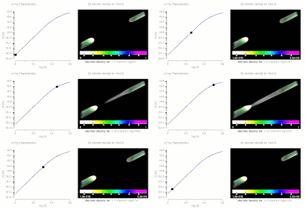
*Transistor — animation hotlinked from Wikimedia Commons (via the Real G.E.N.E.R.A.T.I.V.E. course library, Electronics room). [Details & license](https://commons.wikimedia.org/wiki/File:Threshold_formation_nowatermark.gif).*
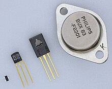
*Transistor — image hotlinked from Wikimedia Commons (via the Real G.E.N.E.R.A.T.I.V.E. course library, Electronics room). [Details & license](https://commons.wikimedia.org/wiki/File:Transistorer_%28cropped%29.jpg).*
> A transistor is a semiconductor device used to amplify or switch electrical signals and power. It is one of the basic building blocks of modern electronics.[1] It is composed of semiconductor material, usually with at least three terminals for connection to an electronic circuit. ([Wikipedia](https://en.wikipedia.org/wiki/Transistor))
<!-- BEAUTY-PASS-MEDIA:END -->
<!-- SIGN-SYSTEMS:START -->
**Semiotic universals** (the notations and alphabet letters this article speaks — each opens its canonical card): circuit symbols iec · flow · saturation · potential · signal. Index: the glyph gallery · SEMIOTICS PORTAL.
<!-- SIGN-SYSTEMS:END -->
## Overview
A **transistor** is a three-terminal [[Semiconductor_device|semiconductor device]] that uses a small [[Signal|signal]] at one
terminal to control a much larger current between the other two. That single property -- a weak
input commanding a strong output -- is what makes it the active element of nearly all modern
[[Electronics|electronics]]: it can **amplify** (a small wiggle in becomes a large wiggle out) and it can **switch**
(a control signal turns the main current fully on or fully off, the basis of every digital logic
gate and memory cell). Invented at Bell Labs in 1947-48 (the point-contact device of Bardeen and
Brattain, then Shockley's more practical **junction transistor**), it displaced the bulky, hot,
fragile vacuum tube and, once it could be etched by the millions onto a single chip, became the
most-manufactured artifact in history. The two great families are the **bipolar junction
transistor** (BJT), controlled by a base *current*, and the **field-effect transistor** (FET /
MOSFET), controlled by a gate *[[Voltage|voltage]]*; the MOSFET dominates digital integrated circuits, while
the BJT remains the cleanest device for learning the underlying idea because its control variable
is a current you can literally count.
This MicroSim illustrates the general transistor through the canonical **bipolar common-emitter
output characteristics** -- the single most recognizable transistor figure. The horizontal axis is
the collector-emitter voltage `V_CE`; the vertical axis is the collector current `I_C`; and the plot
is not one curve but a **family** of them, one for each value of the base drive `I_B`. Each curve
rises steeply out of the origin and then flattens into a near-horizontal plateau: in the flat
region the transistor behaves as a **current source** whose value `I_C = beta * I_B` is set by the
base current and barely depends on `V_CE`. The plateau is not perfectly flat -- it tilts gently
upward (the **Early effect**), so the device has a large but finite output resistance. Reading the
family top to bottom tells the whole story of the device: stack the curves higher by raising
**beta** (the current gain), pick which curve you sit on with **I_B**, and the family is the same
regardless of the circuit around it.
A transistor is never used alone; it drives a load. Connect the collector to a supply `V_CC`
through a resistor `R_C`, and Kirchhoff's voltage law fixes a straight **load line**
`I_C = (V_CC - V_CE) / R_C` across the same axes. The **operating point** `Q` -- the one current and
voltage the circuit actually settles at -- is where that load line crosses the output curve for the
chosen `I_B`. As you raise the base drive, `Q` **walks up the load line**: from the bottom-right
corner (`V_CE ~ V_CC`, `I_C ~ 0`: **cutoff**, the switch is *open*), through the middle of the line
(the **active** region, where the transistor amplifies), to the top-left corner (`V_CE ~ 0`:
**saturation**, the switch is *closed*). Watching `Q` slide between those three regimes -- and
seeing the voltage gain `Av` peak in the middle and collapse at the ends -- is the entire art of
biasing a transistor, captured in one picture you can drag.
## The physics / derivation
**The device: two junctions, one controlled current.** An NPN BJT is a sandwich of an `n`-type
emitter, a thin `p`-type base, and an `n`-type collector, giving two p-n junctions: base-emitter
(BE) and base-collector (BC). In the **forward-active** mode the BE junction is *forward*-biased and
the BC junction is *reverse*-biased. Electrons injected from the emitter into the very thin base
mostly survive the trip and are swept into the collector; only a small fraction recombine and must
be resupplied as base current. The collector current follows the **transport (Ebers-Moll)** law,
exponential in the base-emitter voltage:
```
I_C = I_S * ( exp( V_BE / V_T ) - 1 )
```
where `I_S` is the transport saturation current and `V_T = kT/q ~ 25.85 mV` at room temperature is
the thermal voltage. Because the surviving fraction is nearly fixed by the [[Geometry|geometry]] and doping, the
collector current is a nearly constant multiple of the base current:
```
I_C = beta * I_B I_E = I_C + I_B = (beta + 1) * I_B alpha = I_C / I_E = beta / (beta + 1)
```
`beta` (also written `hFE`) is the **DC current gain**, typically 50-300; `alpha` is just under 1.
This is the heart of the device: a base current of microamps commands a collector current of
milliamps -- a current amplification of `beta`.
**The three operating regions.** Which mode the transistor sits in depends on the two junction
biases, read directly off the output plot:
- **Cutoff** -- both junctions reverse (`I_B ~ 0`): `I_C ~ 0`, `V_CE ~ V_CC`. The device is an
*open switch*.
- **Forward-active** -- BE forward, BC reverse (`V_CE` more than a few tenths of a volt):
`I_C ~ beta * I_B`, almost independent of `V_CE`. The device is a *current source* / *amplifier*.
- **Saturation** -- both junctions forward (`V_CE < V_CE(sat) ~ 0.1-0.2 V`): the collector can no
longer follow `beta * I_B`; `I_C` is limited by the external circuit and `V_CE` collapses to near
zero. The device is a *closed switch*.
**A smooth model for the output characteristics.** To draw the whole family with one continuous
expression (and to find `Q` without case-splitting), the MicroSim uses the standard pedagogical
smoothing of the active/saturation transition multiplied by the Early-effect slope:
```
I_C(V_CE ; I_B) = beta * I_B * ( 1 - exp( -V_CE / V_CEsat ) ) * ( 1 + V_CE / V_A )
```
The factor `(1 - exp(-V_CE/V_CEsat))` rises from 0 at `V_CE = 0` to ~1 within a couple of
`V_CEsat` (the knee, with `V_CEsat ~ 0.2 V`), reproducing the steep climb out of saturation into
the active plateau. The factor `(1 + V_CE/V_A)` is the **Early effect**: extrapolated backward, every
active-region curve aims at the same point `V_CE = -V_A` on the voltage axis, where `V_A` is the
**Early voltage** (here fixed at 80 V). It gives the plateau its gentle upward tilt and the device
its finite **output resistance** `r_o = V_A / I_C`. The model is monotonic increasing in `V_CE`,
which is what lets the operating point be found by a safe bracketed bisection.
**The load line and the operating point.** Put the transistor in a common-emitter stage: emitter to
ground, collector to `V_CC` through `R_C`. KVL around the output loop, `V_CC = I_C * R_C + V_CE`,
rearranges to a straight line in the `I_C`-`V_CE` plane:
```
I_C = (V_CC - V_CE) / R_C
```
with x-intercept `(V_CE = V_CC, I_C = 0)` (the open-switch / cutoff corner) and y-intercept
`(V_CE = 0, I_C = V_CC / R_C)` (the closed-switch / saturation corner); its slope is `-1/R_C`. The
**operating point** `Q = (V_CE,Q , I_C,Q)` is the simultaneous solution of the load line and the
output characteristic for the selected `I_B` -- their intersection. Because the characteristic rises
monotonically in `V_CE` while the load line falls, their difference changes sign exactly once, so
`Q` is found by a fixed-count **bisection** on `V_CE` in `[0, V_CC]` -- no Newton iteration, no
runaway loop. As `I_B` rises, the demanded plateau `beta*I_B` climbs; while it is below the
load-line ceiling `V_CC/R_C`, `Q` sits in the active region with `V_CE,Q = V_CC - I_C*R_C`; once
`beta*I_B` would exceed that ceiling, the transistor **saturates** and `V_CE,Q` clamps near zero.
**Small-signal gain: the amplifier.** Bias the stage in the active region and superimpose a tiny
input. The transistor's **transconductance** is the slope of the exponential at the operating
point,
```
gm = I_C,Q / V_T r_pi = beta / gm r_o = V_A / I_C,Q
```
and the common-emitter **voltage gain** is the transconductance working into the total collector
load (the external `R_C` in parallel with the device's own `r_o`):
```
Av = - gm * ( R_C || r_o ) ~ - gm * R_C = - I_C,Q * R_C / V_T (when r_o >> R_C)
```
The minus sign is the CE stage's signature **inversion**. Notice that `gm*R_C = I_C*R_C/V_T = V_RC/V_T`:
the gain magnitude is just the DC drop across `R_C` measured in units of `V_T (~25.85 mV)`, so it
grows as you push `Q` up the load line -- but you need voltage headroom for the output to swing, so
the textbook compromise biases at `V_CE,Q ~ V_CC/2`. Drive `Q` to either end of the line and the
gain vanishes: at cutoff `gm = 0`, and at saturation there is no `V_CE` left to swing. The MicroSim
draws faint **swing ghosts** at `I_B +/- dI_B` to make this visible: a fixed small base-current
wiggle produces a large `V_CE` excursion `dV_CE = -beta*(R_C||r_o)*dI_B` in the active region, and
almost none at the rails.
## Parameter table (control -> symbol -> range)
| Control | Symbol | Meaning | Range (units) | Default |
|---|---|---|---|---|
| Base-current slider | `I_B` | base drive; selects which output curve (and hence `Q`) is active; `I_C = beta*I_B` | 0 - 120 uA | 40 uA |
| Current-gain slider | `beta` (`hFE`) | DC current gain `I_C/I_B`; sets the vertical spacing of the curve family | 20 - 400 | 150 |
| Supply slider | `V_CC` | collector supply voltage; load-line x-intercept | 1 - 15 V | 10 V |
| Load slider | `R_C` | collector resistor; load-line slope `-1/R_C` (log scale) | 100 ohm - 10 kohm | 1 kohm |
| Reset button | -- | restore ALL controls to defaults | -- | -- |
Fixed model constants: thermal voltage `V_T = kT/q = 25.85 mV` (T = 300 K), Early voltage
`V_A = 80 V` (sets the plateau tilt and `r_o`), knee scale `V_CEsat = 0.2 V`, and a small-signal
base-current excursion `dI_B = 4 uA` for the swing ghosts.
Derived / read-out quantities: the active-region collector current `beta*I_B`; the operating point
`Q = (V_CE,Q , I_C,Q)` at the load-line / curve intersection; the load-line corners (open-switch
`V_CE = V_CC`, closed-switch `I_C = V_CC/R_C`); the voltage drop `V_RC = I_C*R_C`; the region label
(cutoff / active / saturation, with the switch/amplifier reading); the transconductance
`gm = I_C/V_T`; the output resistance `r_o = V_A/I_C`; the small-signal voltage gain
`Av = -gm*(R_C||r_o)`; and the collector power dissipation `P_C = V_CE,Q * I_C,Q` (largest mid-line,
the reason a switching transistor runs coolest fully on or fully off).
## Learning objective
Predict, from `I_C = beta * I_B` and the load line `I_C = (V_CC - V_CE)/R_C`, **where the operating
point `Q` sits** for a given base drive, and explain how raising `I_B` walks `Q` up the load line
through the three regions -- **cutoff** (open switch, `I_C ~ 0`), **active** (amplifier,
`Av = -gm*(R_C||r_o)` largest near mid-line), and **saturation** (closed switch, `V_CE ~ 0`) -- so
that the same device serves as both a linear amplifier and a digital switch depending only on its
bias.
<!-- CRAFT-LINK:START g12 -->
*Built to the [[WT!P5_js_Microsim_Master_Class|p5.js Master Class]].*
<!-- CRAFT-LINK:END -->
<!-- SPINEPATH:BEGIN g20 — shortest chain of Wikipedia links between local articles to a Compendium Main article; do not hand-edit inside -->
*Connected to the Apex Spine:* Transistor → [[Silicon_dioxide|Silicon dioxide]] → [[Properties_of_water|Properties of water]] — [[WT!Thury_Hydrodynamics_Compendium|Compendium]] section 6, *Water*.
<!-- SPINEPATH:END -->
<!-- ELECSIM:BEGIN g28 — Electronics portal microsim (framework build, specs/sims/Transistor.json); do not hand-edit inside -->
**Microsim — three.js (Wikitube framework):** *The transistor: output characteristics and the load line*
<div class="wt-sim" data-src="https://wikitube-3d-microsims.netlify.app/electronics/Transistor.html" data-title="Transistor"></div>
*Built from `MICROSIM_GUIDE/specs/sims/Transistor.json`; part of the [[Electronics]] set ([[PORTAL_Electronics]]).*
<!-- ELECSIM:END -->
## Wikipedia : Wikitube
**Strict pair:** [Wikipedia](https://en.wikipedia.org/wiki/Transistor) : [Wikitube](https://en.wikitube.io/wiki/Transistor)
## Previous hub tags
Tree parent: [[Information_theory]].
Legacy hubs: `ENGINES`.
---
*Sources: 2 legacy notes. Minted wave 1, 2026-07-30 (v1.6 order).*